5 Recent Breakthrough Innovations in Biotechnology
The field of biotechnology is constantly advancing. From finding ways to slow down the process of food spoilage, advancements in genetic engineering, to adapting organisms to clean up contaminated environments, new applications and biotechnological inventions are continuously being developed to help improve our world. Here are five breakthrough biotechnological innovations currently underway.
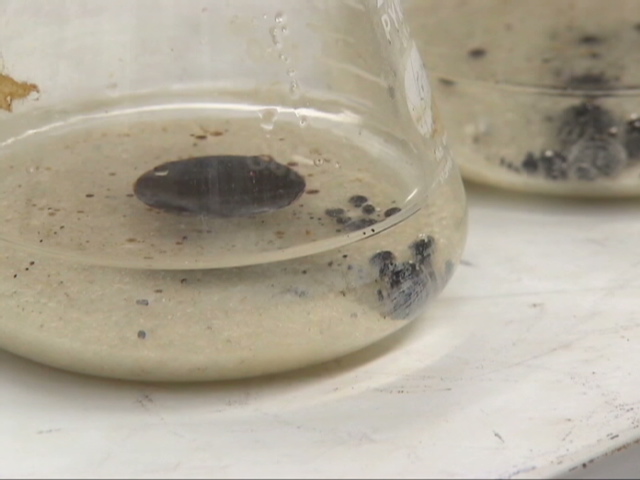
Oil-Eating Bacteria to Clean up Oil Spills
(Image:Source)
The oil-spill has been one of the biggest issues the environmental, health, agricultural and financial sectors have been tackling, and scientists in Europe have sequenced the genome for an oil-eating bacterium, which could lead to faster, more efficient ways to clean up oil spills.
The oil-spill has been one of the biggest issues the environmental, health, agricultural and financial sectors have been tackling, and scientists in Europe have sequenced the genome for an oil-eating bacterium, which could lead to faster, more efficient ways to clean up oil spills.
That certain bacteria have the ability to metabolize oil isn’t a new discovery of course. Back in 1989, bacteria were used experimentally in attempts to clean up the 11 million gallons of crude oil spilled by the Exxon Valdez after it ran aground off the coast of Alaska. Though it made little to no difference back then, now that researchers have a complete blueprint for the oil-hungry bacteria:Alcanivorax borkumensis, they’ll have the ability to optimize the conditions for these bugs, enabling them to soak up the hundreds of millions of liters of oil that enter our waters each year.[Source]
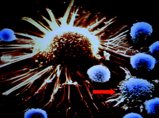
Tumor-Fighting Immune Cells to Attack Cancer
(Image: Source)
Researchers at UCLA’s Jonsson Comprehensive Cancer Center have created a large, well-armed troop of tumor-seeking immune system cells to locate and attack dangerous melanomas. Dr. Antoni Ribas, the senior author of the study says: “We’re trying to genetically engineer the immune system to become a cancer killer and then image how the immune system operates at the same time.”
Researchers at UCLA’s Jonsson Comprehensive Cancer Center have created a large, well-armed troop of tumor-seeking immune system cells to locate and attack dangerous melanomas. Dr. Antoni Ribas, the senior author of the study says: “We’re trying to genetically engineer the immune system to become a cancer killer and then image how the immune system operates at the same time.”
In the study, melanomas grown in mice used an inactive HIV-like virus to serve as a vehicle to arm the lymphocytes with T cell receptors, which caused the lymphocytes to become killers of cancerous cells. A reporter gene, which glows “hot” during PET scanning, was also inserted into the cells which helps researchers track the genetically engineered lymphocytes after they get injected into the blood stream, make their way to the lungs and lymph nodes, and then home in on the tumors wherever they may be located within the body. The team created and injected about one million genetically engineered lymphocytes into a mouse but say that in humans, the number of tumor-seeking cells needed to fight the cancer is approximately one billion. The researchers say, if all goes well, human studies of the process could begin in approximately one year. [Source]
Engineered Tobacco Plants as Biofuel

(Image: Source)
Finally putting tobacco plants to good use, researchers from the Biotechnology Foundation Laboratories at Thomas Jefferson University have identified a way to increase the oil in tobacco plant leaves, with the aim of using it as biofuel. This is a promising prospect, one, because it offers an alternative to exploiting plants that are used in food production, and two, because tobacco plants generate biofuel more efficiently than other agricultural crops.
Finally putting tobacco plants to good use, researchers from the Biotechnology Foundation Laboratories at Thomas Jefferson University have identified a way to increase the oil in tobacco plant leaves, with the aim of using it as biofuel. This is a promising prospect, one, because it offers an alternative to exploiting plants that are used in food production, and two, because tobacco plants generate biofuel more efficiently than other agricultural crops.
The challenge researchers faced was that this precious oil is mostly found in tobacco seeds, and tobacco plants only produce about 600 kg of seeds per acre. However, they have now found ways to genetically engineer the plants so that their leaves express more oil. According to one of the project’s researchers, Dr. Andrianov, they have been able to modify plants to produce 20-fold more oil in the leaves. Andrianov says “”Based on these data, tobacco represents an attractive and promising ‘energy plant’ platform, and could also serve as a model for the utilization of other high-biomass plants for biofuel production.” [Source]
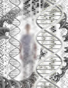
Cheap, Effective Genome Sequencing Technology
(Image: Source)
Personalized healthcare is increasingly being applied to develop more effective treatments for disease and prevent a wider variety of conditions. Genome sequencing is one the most critical tools for personalized medicine, as it provides the individual genetic information necessary for the effective diagnosis and targeted treatment of particular diseases. Last month, a new collaborative agreement between Roche, a leader in biotechnology and research-focused healthcare, and IBM, one of the world’s largest technology companies, has them joining forces to develop a nanopore-based sequencer that will directly read and decode human DNA quickly, efficiently and affordably.
Personalized healthcare is increasingly being applied to develop more effective treatments for disease and prevent a wider variety of conditions. Genome sequencing is one the most critical tools for personalized medicine, as it provides the individual genetic information necessary for the effective diagnosis and targeted treatment of particular diseases. Last month, a new collaborative agreement between Roche, a leader in biotechnology and research-focused healthcare, and IBM, one of the world’s largest technology companies, has them joining forces to develop a nanopore-based sequencer that will directly read and decode human DNA quickly, efficiently and affordably.
Similar to vps hosting offering affordable shared hosting, their goal is to reduce the cost of sequencing an individual’s genome to between $100 and $1000.Currently, companies such as San Diego’s Illumina, which specializes in array-based solutions for DNA, RNA and protein analysis, charge anywhere from $9,500-$19,500, an already drastic drop compared to its previous $48,000 price tag.
In order to reduce the cost so significantly, the new partners want to be able to perform true single molecule sequencing, that will decode molecules of DNA as they are threaded through a nanometer-sized pore in a silicon chip. This approach should deliver significant advantages in cost, throughput, scalability, and speed compared to other sequencing technologies currently available or in development. [Source]
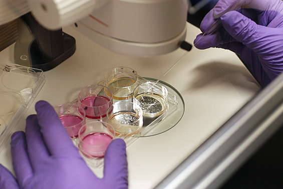
Stem cell culturing without the use of animal substances
(Image: Source)
Researchers at Sweden’s Karolinska Institutet, one of Europe’s largest medical universities, have managed to produce human stem cells without the use of other cells or substances from animals, in a completely chemically-defined environment. Embryonic stem cells have, up to this point, been cultured with the help of proteins from animals, ruling out the possibility of using them for treatment on humans. Now, they are cultured on a matrix of a single human protein: laminin-511, a part of our connective tissue that acts as a matrix that our cells can attach to. The possibilities are tremendous thanks to this scientific breakthrough that will give scientists the ability to develop different types of cells, which can be tested for the treatment of various human diseases. [Source]
Researchers at Sweden’s Karolinska Institutet, one of Europe’s largest medical universities, have managed to produce human stem cells without the use of other cells or substances from animals, in a completely chemically-defined environment. Embryonic stem cells have, up to this point, been cultured with the help of proteins from animals, ruling out the possibility of using them for treatment on humans. Now, they are cultured on a matrix of a single human protein: laminin-511, a part of our connective tissue that acts as a matrix that our cells can attach to. The possibilities are tremendous thanks to this scientific breakthrough that will give scientists the ability to develop different types of cells, which can be tested for the treatment of various human diseases. [Source]


